What is cutting? In the semiconductor assembly process, there are various processes that involve cutting. In our process, the term "cutting" is used to refer to two types of processes: "stamping," in which a thin metal plate called a lead frame, which is the foundation of an IC package, is cut with a die; and "molding," in which a lead frame, polyimide substrate, or other material is sealed with resin and then cut into individual pieces into the final product shape.
What is bending molding? In the semiconductor assembly process, "bending" is one of the processes to form the product into the final product shape after placing the semiconductor chip on the lead frame substrate, connecting the semiconductor chip to the substrate terminals with gold wire, and resin sealing (molding) the surrounding area with epoxy resin. There are two types of final product shapes: lead foot cutting molding and lead foot bending molding, and "bending molding" refers to lead foot bending molding. In the semiconductor industry, foot trimming is called "trimming" and foot bending is called "forming.
Features
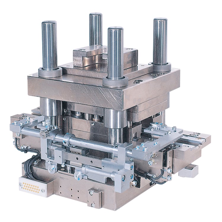
Lead cutting Appropriate clearance setting during lead cutting realizes cutting quality (proper shear and fracture surface) and narrow pitch (0.35 mm) lead cutting.
Oil-free cutting (dry cutting) enables simultaneous cutting of lead and resin, as well as cutting quality (proper shear and fracture surface) of glass epoxy substrates.
Bending molding In response to the demand for improved bending quality, we have developed a bending method that minimizes contact marks through the use of a special mold concept and ideal contact with the lead.
In addition to minimizing contact marks, the use of this bending method reduces contamination of the mold by the material, enabling high-quality bending with less maintenance.