.jpg?width=750&height=715&name=YSB55w%E5%8F%97%E6%B3%A8%E7%B5%82%E4%BA%86(E).jpg)
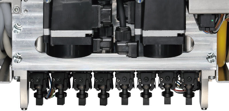
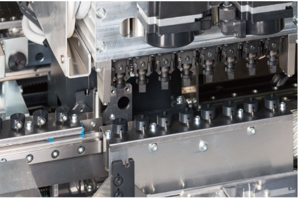
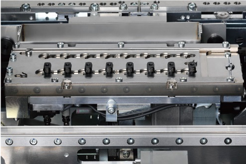
1.Dual bonding heads Multi-nozzle (8 nozzles per head)
Two 8-nozzle heads with compact design enable high precision force control and also support thin die processing.
2.Dual flip heads
Achieves high-speed pick-up by parallel processing with 2 flip heads.
3.Multi-die supply
Equipped with 2 supply units for each flip head unit. Feeds flip chips with no time loss!
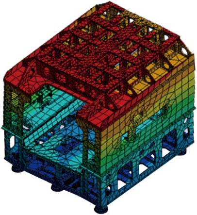
1.High rigidity frame & beam
Meticulous structural analysis and test verification achieve both high-level accel-decel drive and high-precision.
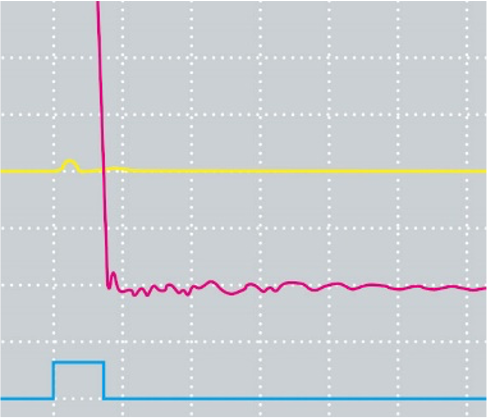
2.Linear motor/driver designed in-house
Unique dedicated design gives high-speed along with superb positioning accuracy.
*Example of measurement results with shaft-spindle stopped
3.High resolution chip recognition camera
Missing bump check and precise position alignment using bump positions.
4.Maintaining high placement accuracy
Our in-house developed MACS (Multiple Accuracy Compensation System) has been upgraded and now achieves bonding accuracy ±5μm (3σ). Original heat analysis & heat compensating algorithm realizes consistent placement accuracy.
1.Newly developed dipping station
Tool-less/skill-less flux thickness setting saves product change-over time drastically.
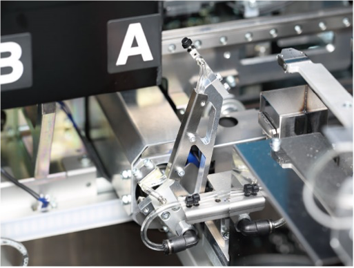
2.Nozzle station (ANC : Auto Nozzle Change)
Auto nozzle changer handles chip size range from □2 to 30mm minimizing product change-over time.
*Example of measurement results with shaft-spindle stopped
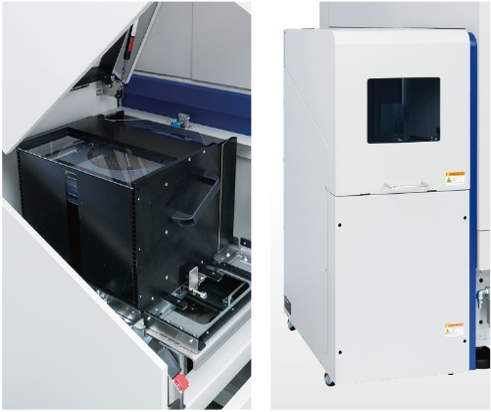
3.Wafer feed unit
Wafer feeder with wafer expander & theta alignment mechanism as standard feature.