.png?width=750&height=750&name=SPA-1000%E8%B2%A9%E5%A3%B2%E7%B5%82%E4%BA%86(E).png)
Overview
High-Accuracy Twin-Head Die Bonder
One type of die bonder. A highly productive, space-saving, high-precision die bonder with dual bonding heads. The machine heats an automatically fed substrate and performs DAF* bonding. After automatically feeding diced wafer, wafer mapping and reject mark recognition are performed, and an appropriate die is picked up by the transfer head. The machine transfers the die to the die precisor stage and then to the pickup point of each bonding head for feeding. Bonding is performed based on the results of substrate recognition, die precisor stage die recognition, and die backside recognition (option). The bonded substrate is unloaded to the unloader magazine.
*DAF: Die Attach Film
Features
- High-accuracy bonding by unique 3D-NRS(Non-Reaction Servo system) technology
- High-productivity and space-saving footprint by adopting twin-head
- High-speed thin die pick-up system with a speed of 400ms / t:20um(option) *Depending on material conditions
- Friction-free bonding head with simultaneous positional and force control for thin die stacked devices
- Cleanness control with HEPA-filter and stainless steel full cover
- Equipped with die back-side camera on each bonding head, enhancing inspection function with a total of 8 cameras
- Capable of handling large substrates up to 120mm width x 300mm length
Usage examples
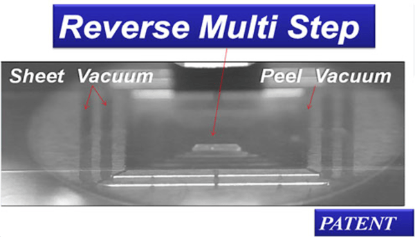
Handling ultra thin die for bonding: Pulse Vacuum Reverse Multi Step (PV-RMS)
The thickness of multilayered NAND flash memories has been reduced to less than 30 um including an adhesive layer. Although silicon is a relatively hard material, it will bend readily and break easily at this thickness. In making a device, a die pickup technique is necessary, but it is extremely difficult to remove an ultra thin die attached to the wafer tape.
You may have experienced that peeling off a bandage quickly caused pain. Alleviating this pain is compared to the function of Pulse Vacuum-Reverse Multi Step (PV-RMS) that picks up thin dies from wafer tape. By pulsing vacuum from the outside of wafer tape, the PV-RMS promotes peeling of the die while reducing the adhesive force – corresponding to the reduced pain that would result from a similar method of bandage removal. It is effective not only for thin dies but also for dies with a fragile TSV structure. This is a key technique for future electronic device packaging.

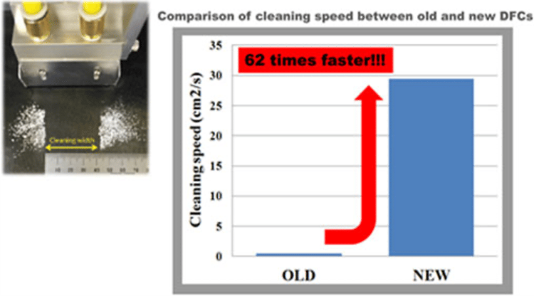
Cleaning before connecting is important: Dust Free Cleaner (DFC)
Die Attach Film (DAF), an adhesive used for NAND flash memories, is as thin as 5 um. The NAND flash memories are often stacked in multiple stages. When a new die is stacked, if fine particles of 5 um or more are present on an object to be bonded, die cracking may occur and the productivity may decrease. Cleaning before die stacking is, therefore, an essential factor for successful multi-stack bonding.
Shinkawa was among the first to address this issue and developed a dust free cleaner (DFC) unit, which has a cleaning speed 60 times faster than the conventional model. Its high-speed cleaning capability is recognized by the industry’s leading manufacturers as a contributor to total productivity improvement.
In addition to DFC, Shinkawa will strive to develop technologies related to cleanliness control and provide tools to increase customers' productivity.

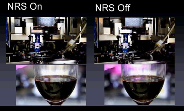
3D-NRS Technology: (three-dimensional non reaction servo system)
In order to ensure bonding accuracy and increase productivity, it is necessary to reduce mutual interference due to vibration of the drive units. In the SPA-1000, the 3D-NRS technology controls vibration of the two high-speed bonding heads, enabling high productivity as well as high precision. The model has bonding accuracy of XY±5 µm (3σ) and θ±0.05° (3σ), achieving twice the UPH of a conventional model.

Promotional Video
Product Specifications
ITEM | DETAILS |
---|---|
Product Name | Die Bonder |
Model | SPA-1000 |
Bonding Method | DAF bonding |
Accuracy | XY:±5μm (3σ)、θ:±0.05°(3σ) (Machine accuracy excluding material-induced factors) |
Productivity | The productivity increased by 2.5 times compared with conventional model. (Theoretical value with Shinkawa's standard sample) |
Chip Size | □0.8~25mm |
Wafer Size | Maximum 12-inch |
Substrate/Leadframe Size | Width |
Options Available | Thin die application kit, Film attachment unit, capability to handle overhead transport (OHT) |
Utilities | Input Power Supply Single Phase AC200V±5% 50/60Hz (Other power supply options available on request) Power Consumption Maximum 3.2 kVA (3.2kW) Air 500kPa(5kgf/cm2)900 L/min Vacuum Below -74kPa (-550mmHg) (gage) |
Physical Dimensions and Mass | Approx. 2,280W × 1,510D × 1,670H mm Approx. 2,300 kg (excludes monitor display and signal tower)※Configuration and specifications of this machine are subject to partial modification without prior notice. |
*Configuration and specifications of this machine are subject to partial modification without prior notice.