Bump Bonder
SBB-5200

Bump Bonder

selling agency

SHINKAWA LTD.

Overview

Wide-area Adaptive High-speed Wafer Bump Bonder

Features

  • High-speed bonding of 30 ms/bump based on Wire Bonder model UTC-5000
  • Capable of handling up to 6-inch wafers by incorporating wafer rotary stage
  • Equipped with Two wafer stages with temperature up/down control function, reducing time for SAW filter wafer changeover and increasing productivity
  • Automatic free air ball monitor function (FAM) measuring initial ball diameter
  • Wafer autoloader enables automatic wafer replacement (option)

Usage examples

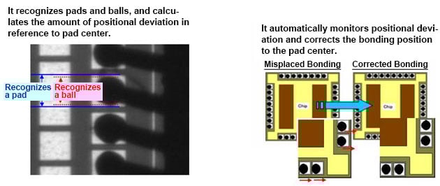
Bond Inspection Measurement (BIM)

BIM is the capability to correct bonding position by feedback of the positional deviation of each bonding position from the pad center using images captured after bonding. It corrects in real time any positional deviation due to disturbances during the bonding operation, and stabilizes the bonding accuracy.

SBB-5200-1

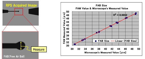
Free Air Ball Measurement (FAM): Automatic free air ball size monitoring capability

FAM is a unique technology of Shinkawa which monitors free air ball (FAB) diameter during wire bonding, and detects its abnormality at the same time, to stabilize the diameter. To detect abnormality, the function to monitor capillary tip position – called Reference Positioning System (RPS) – is utilized. FAM is a key technology to support the highly reliable bonding of the UTC-5000 series.

SBB-5200-2

Product Specifications

ITEMDETAILS
Product NameBump Bonder
ModelSBB-5200
Bonding Accuracy±2.5 μm(3σ)Using Shinkawa standard device
Correction of Bonding PositionSystem to check and correct capillary offset prior to bonding through Shinkawa RPS
Bonding Speed30 ms/ bump (no reverse motion)  using Shinkawa standard device
ResolutionXY-table: 0.1 μm  Z-axis: 0.1 μm
Vibration ControlShinkawa NRS - Non Reaction Servo System
Bonding AreaMaximum φ150 mm (6-inch wafer)
Wire SizeAu φ15~32 μm
Bonding ForceMaximum 4.9N
No. of Bonding Bumps30,000 bumps maximum
Wafer Stage2 wafer stages for 6-inch wafers ※with temperature up/down control function
Wafer SizeSize
Maximum 6 inches
(Conversion parts are required when wafer size changes.)

Thickness
0.15~0.6 mm(Conversion parts may be required when wafer thickness changes.)
Production ManagementManagement of equipment availability through production management monitoring screen
Options AvailableAutomatic wafer loader for 6-inch wafer
UtilitiesInput Power Supply
Single Phase 100 VAC (±5% input variation)
50/60Hz (other voltage requires transformer)
Power Consumption
Approx. 1.1kVA

CDA
500 kPa(5 kgf/cm2)100 L/min

Vacuum
-74kPa or below (-550 mmHg) (gauge)
Physical Dimensions and Mass1,000W × 1,084D × 2,092H mm  Approx. 500 kg

*Configuration and specifications of this machine are subject to partial modification without prior notice.

Installation dimensions

Contact Us

For products and various inquiries, click here.

List of inquiries