
Overview
- Chip-to-Wafer package bonder for TCB process
- Capable of switching to Chip-to-Substrate bonding for TCB process within short period of time
- Capable of handling face down process (face up process as an option)
- Capable of handling several kinds of processes such as TCB (NCP/NCF/TC-CUF), C2 and C4, and FO-WLP
Features
- High-accuracy bonding achieved by adopting the unique Non-vibration System (NVS) technology
- Capable of handling high force up to 350N with Force Free Gantry (FFG)
- High throughput achieved by short heating and cooling time with high-speed pulse heater
- Process monitoring and management function securing stable quality and process portability
- Flexibility to handle various plunge-up systems, enabling thin die handling
- Automatic product-type changeover function with capability to bond up to 4 different product-type chips, enabling 2.5D and 3D stack packaging
- High-productivity and space-saving footprint by adopting multiple heads
- Flexible support for the following options:
1. Supporting face-up process
2. Mounting TCB for large chips (□35mm)
3. Transferring and applying FLUX material to chips
4. Supporting chip feed from tape reel
5. Supporting base wafer feed by OHT
Usage examples
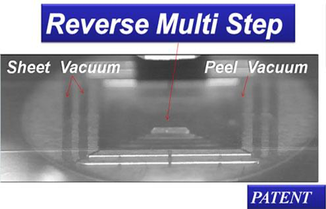
Handling ultra thin die for bonding: Pulse Vacuum Reverse Multi Step (PV-RMS)
The thickness of multilayered NAND flash memories has been reduced to less than 30 um including an adhesive layer. Although silicon is a relatively hard material, it will bend readily and break easily at this thickness. In making a device, a die pickup technique is necessary, but it is extremely difficult to remove an ultra thin die attached to the wafer tape. You may have experienced that peeling off a bandage quickly caused pain. Alleviating this pain is compared to the function of Pulse Vacuum-Reverse Multi Step (PV-RMS) that picks up thin dies from wafer tape. By pulsing vacuum from the outside of wafer tape, the PV-RMS promotes peeling of the die while reducing the adhesive force – corresponding to the reduced pain that would result from a similar method of bandage removal. It is effective not only for thin dies but also for dies with a fragile TSV structure. This is a key technique for future electronic device packaging.

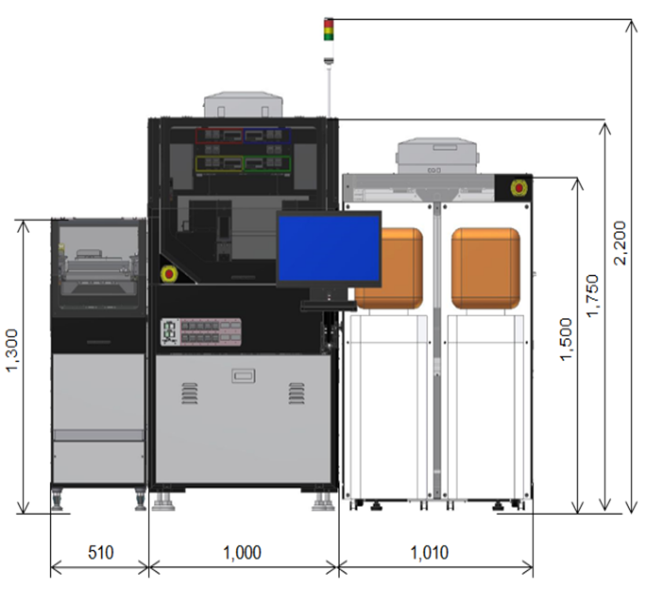
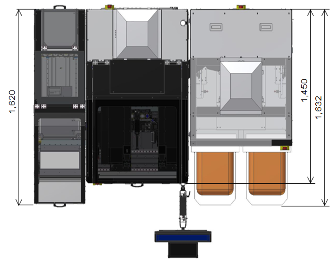
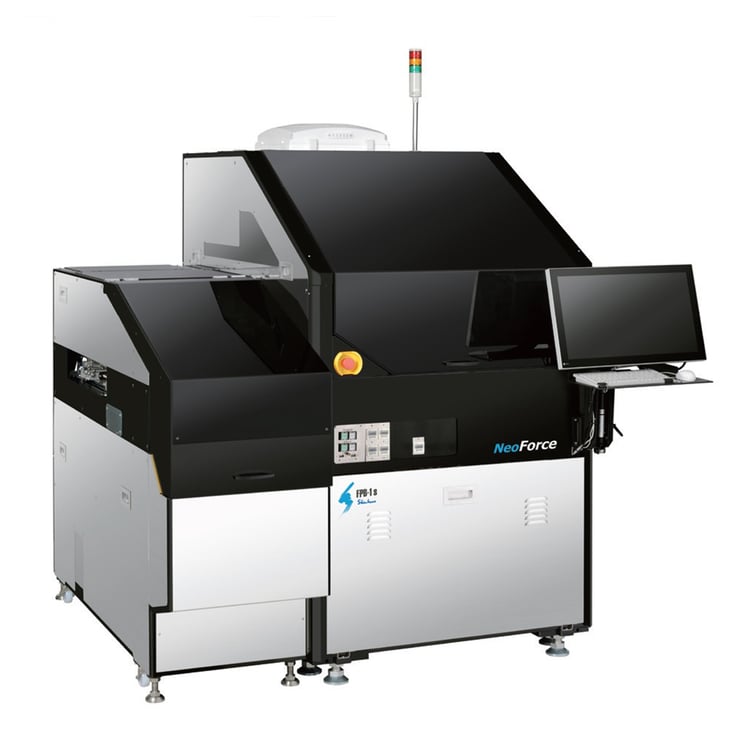
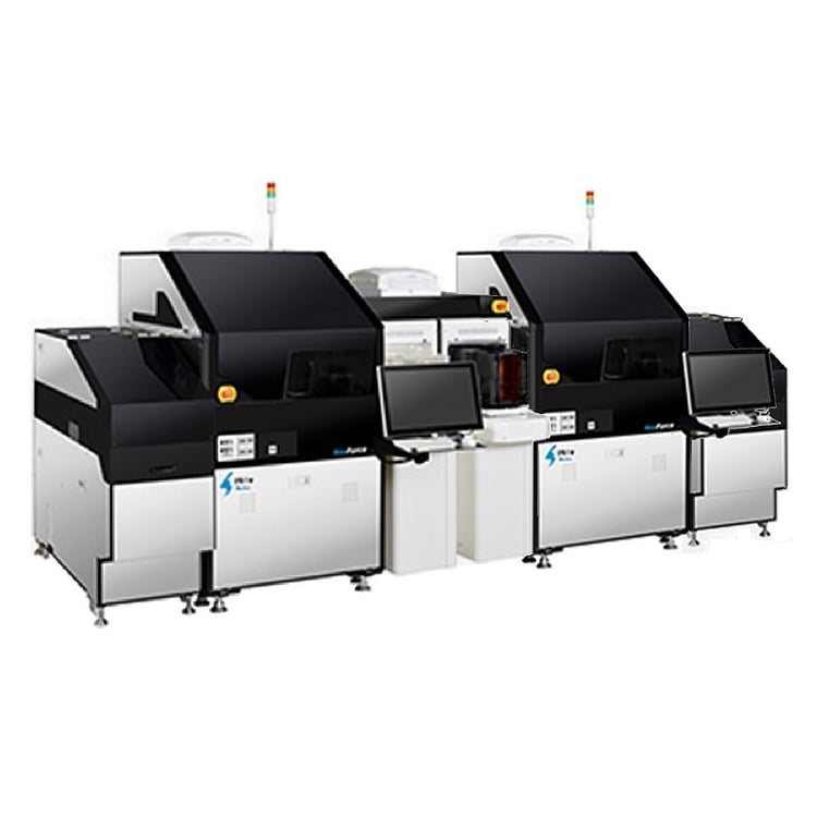
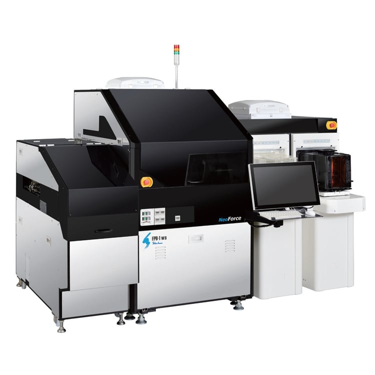
Connect efficiently: Flip-chip Collective-bonding
As dies become larger, thinner and more densely populated with interconnects, reduced die warpage and increased die placement precision are required during flip chip bonding. To address this issue, the thermal-compression bonding (TCB) process has been proposed. It has been used in the latest memories manufactured by the through-silicon-via (TSV) process such as high bandwidth memory (HBM) and hybrid memory cube (HMC). Thermocompression bonding enables simultaneous solder bonding of interconnects and curing of underfill. However, the thermocompression bonding process requires a cycle time of about 10 seconds, which limits the improvement of productivity. Shinkawa conducts basic research and develops sub-system technologies applicable to various methods for collective bonding of multiple dies such as gang-bonding. We reported at the Electronic Components and Technology Conference (ECTC) 2017 that productivity can be improved up to 20 times by a combination of optimized sub-system technologies and usage of the high-speed TCB bonder FPB series.

Promotional Video
Product Specifications
ITEM | DETAILS |
---|---|
Product Name | Package Bonder |
Model | FPB-1ws NeoForce |
Bond Process Handling Capability | TCB (NCP/NCF/TC-CUF), C2 and C4, FO-WLP |
Bonding Accuracy | ±2.5 μm(3σ) Based on bonding conditions at Shinkawa |
Machine UPH | UPH6,000 (C4 mode / process time not included) Based on bonding conditions at Shinkawa |
Bonding Force | 0.3–350N ※Capable of selecting bond force control method at bonding process However, it is not capable of switching over between low force control and high force control in the identical bond profile ・Low force control mode:0.3–20N ・High force control mode:10–350N |
Bonding Tool Setting Temperature | RT – 400℃ (1℃/Step, Pulse heat) |
Bonding Stage Setting Temperature | RT–200℃ (1℃/Step) |
Chip Size | □1 – 22mm t=0.02 – 0.7mm (Contact us for □22mm or larger, options, or other conditions) |
Chip Wafer Size | φ200mm, φ300mm |
Base Wafer Size | φ300 mm (φ200 mm Option) /Substrate |
Bonding Direction | Face down/Face up (Option/Other conditions available on request) |
Options Available | Communication interface SECSⅡ, HSMS and GEM |
Utilities | Input Power Supply Single Phase AC200V–240V±5% 50/60 Hz (Other power supply options available on request) Power Consumption Maximum 14.0kW Air 570kPa(5.7kgf/cm2)300L/min Connection: φ10 Tube × 3 spots Vacuum Below -75kPa (-550mmHg) (gage) Connection: φ10 Tube × 3 spots |
Physical Dimensions and Mass | Approx. 2,520W × 1,620D × 1,750H mm Approx. 3,100kg (excludes monitor display and signal tower) |
*Configuration and specifications of this machine are subject to partial modification without prior notice.